Stack up
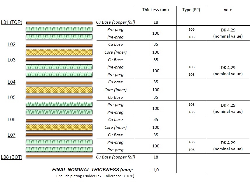
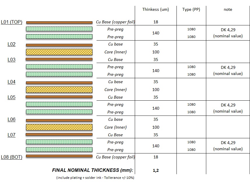
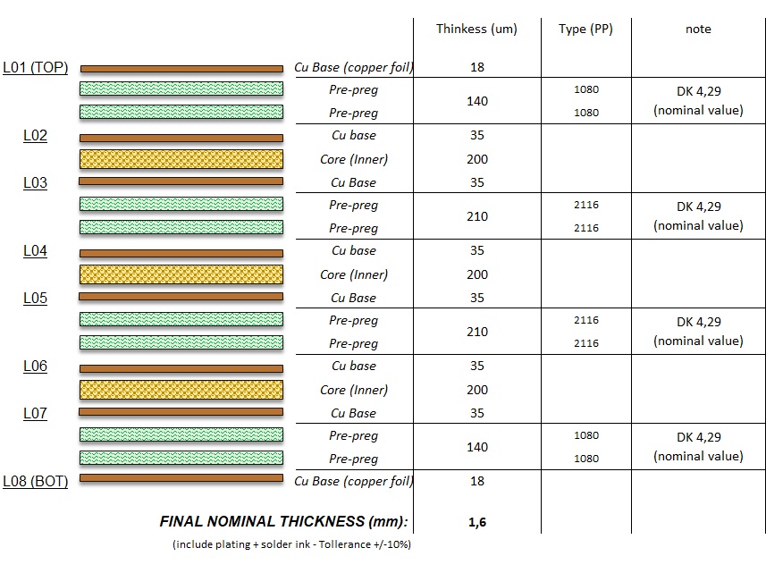
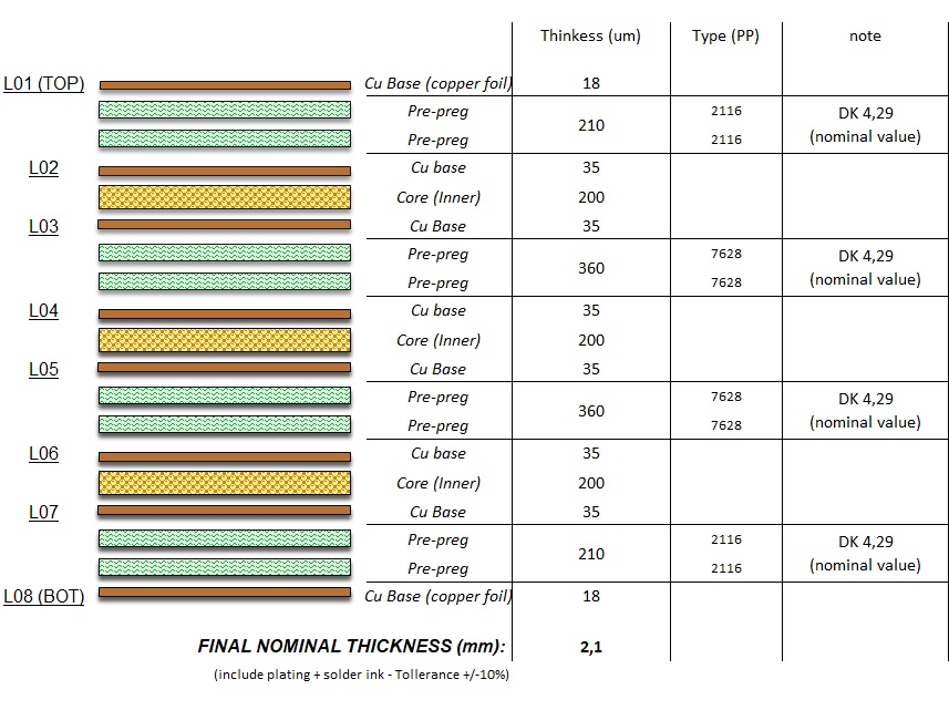
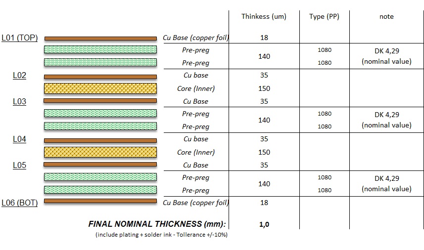
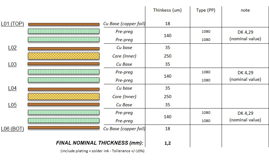
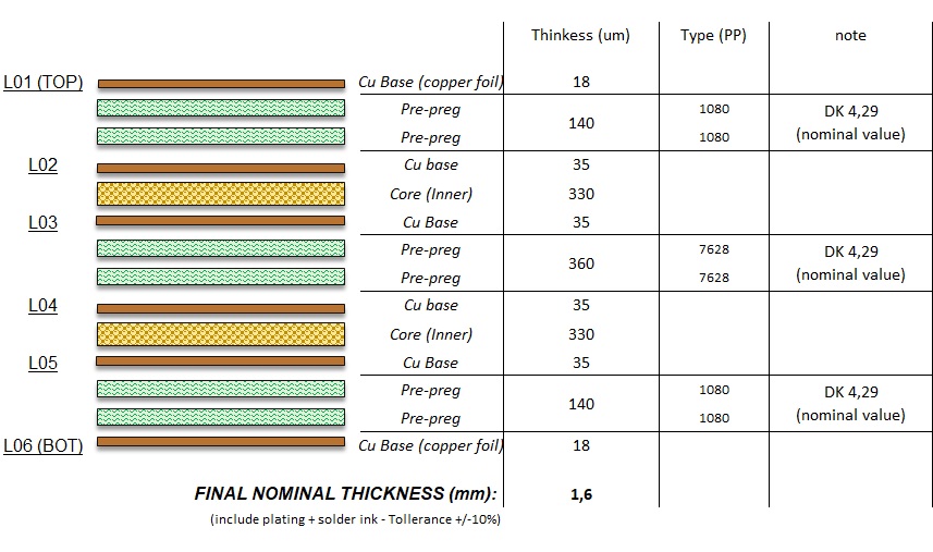
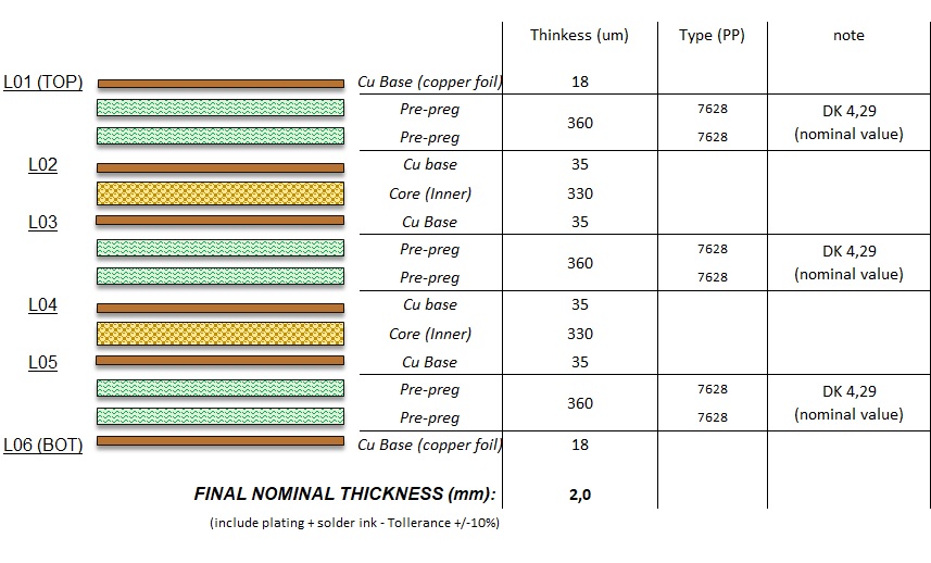
Displays stack-up variations based on number of layers and thickness
-
GUARDA IL VIDEOGUARDA IL VIDEO
SCOPRI IL VIDEO
Multilayer printed circuit boards contain more than 2 copper layers. We differ between outer and inner layers, which are connected and pressed together according to a defined layer structure.
The layer structure basically consists of the following elements:
- Copper foil
- Prepregs (glass/resin laminate)
- Material core (2 copper foils and prepregs pre-pressed)
The sequence of the individual layers depends on the materials and prepregs available and on the designer’s specifications. We call this arrangement layer stackup.
Important specifications for the layer structure include
- Copper thickness of all layers
- Total thickness of the printed circuit board
- Insulation distances between copper layers (e.g. for controlled impedances)
Below you will find the most common layups for multilayers of different thicknesses from 4-8 layers based on the available storage materials. All stackups are shown with a copper thickness of 18µm, but can be realized in the same way with 35µm base copper. Higher copper thicknesses affect the stackup and the final thickness.
For special requirements with individual layer stackup, our technical team will be happy to advise you at any time.
It should be noted that at least 2 layers of prepreg must always be used in order to obtain sufficient filling of the structures and uniform symmetry in the buildup.
2 layers


4 layers
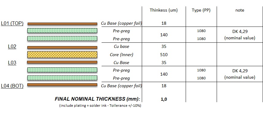
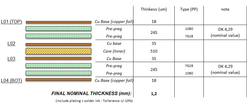
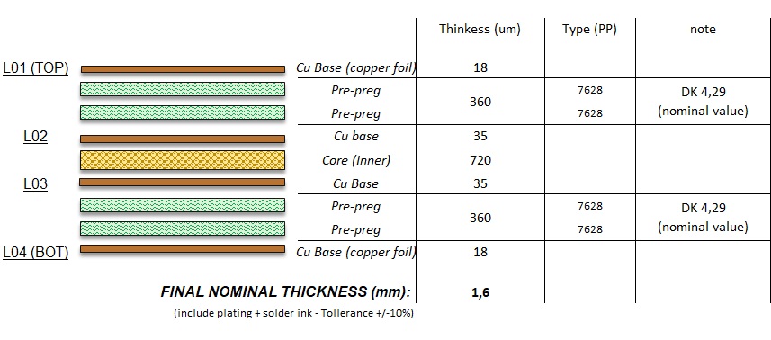
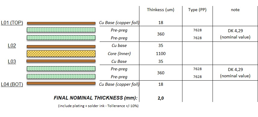
6 layers
8 layers
